


")


 The LM3886 circuit is in a non-inverted configuration, so the input impedance is determined by the input resistor R1, i.e. 47k. The 680 ohm and 470pF resistor capacitor filter network is used to filter out the high frequency noise at the RCA input. The 220pF C4 and C8 capacitors are used to shot out the high frequency noise at the LM3886 input pins.


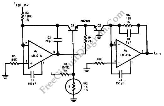 Anti-Log Converter Schematic Circuits
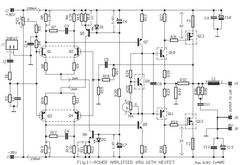 65W Power Amplifier Circuits with HEXFET


 Audio Amplifer Circuit 230W With MOSFET IRFP240,9240


 Commercially available hearing aids are expensive. Here is a cheap hearing aid circuit that uses only four transistors and some passive components. In moving the power switch S to on position, the condenser microphone detects the sound signal, which is amplified by transistor T1 and T2.


These
multi-frequency signals are mixed and fed to the audio amplifier built
around IC LM386. The output of IC2 is fed to the speaker through
capacitor C9. If you want louder sound, use power amplifier TBA810 or
TDA1010. Only five outputs of IC1 are used here as the other five
outputs (pins 4 through 7 and 14) produce ultrasonic signals, which are
not audible. Assemble the circuit on a general-purpose PCB and enclose
in a suitable cabinet. Regulated 6V-12V (or a battery) can be used to
power the circuit.


 The main function of the tuner is to select the RF signals from the desired frequency spectrum wave on VHF and UHF and more signs in the air Changing RF variable into a fixed IF frequency and to provide sufficient strengthening to cover the original data that has been transmitted.


