Showing posts with label rf. Show all posts
Showing posts with label rf. Show all posts
Saturday, November 16, 2013
RF AF signal detector

The series that we will make this is a special electronic circuit can be used to detect the presence or absence of signal AF / RF. The circuit is very neat and simple to make. Costs it takes quite cheap. If you are already assembling this circuit, then with easy reader determine whether there is AF or RF signal at a particular section of a circuit.
Basic circuit uses an audio amplifier and a loudspeaker with switch input for AF and RF signals. The whole device can be made small as possible so it can be included in a container to maintain security. Audio amplifier section in this series created by IC TDA 2822M, with low stereo power amplifier in 8-pin mini-DIP. IC is used as a bridge cofiguration to shrink to 250 mW output power, loudspeaker handle 4 ohm, 500mW. The current required is less than 10mA with voltage of 3V battery.
 |
| RF-AF signal detector schematics |
How it Works circuit
When the selector switch in the AF position, working on the input audio signal AF amplifier input (pin 7 of IC 1) through a capacitor C2 and potentiometer VR1. Capacitors C2 always hold input amplifier of the DC voltage and make it happen in the audio signal frequency. Input Signal IC 1 can be arranged with the help of potentiometers VR1.
When the selector switch in position RF and demodulator detector circuit formed by capacitor C1, diode D1, and resistors R1 and R2 are connected to the input The set. When the audio signal is detected then it will actually go kerangkaian to be strengthened. Signal detection is done by plugging probe (probe) on the legs of the existing components.

Friday, October 25, 2013
RF power amplifier IC
RF power amplifier IC is a type of electronic amplifier used to convert low-power radio frequency signal into a larger signal strength is important, usually for driving a transmitting antenna. This is usually optimized for high-efficiency, high output power (P1dB) of compression, loss of income on the input and output, better benefits, and optimal heat dissipation.
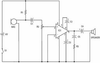 |
| RF power amplifier IC |
To make our amplifiers can also use transistors or IC OP Amp. In the op amp is actually a transistor that is in the form of a series so its easier to use.
Suppose that is used in the amplifier IC Op Amp 741 is a monolithic high performance electronic components that use Fairchild epitacial process. IC Op Amp 741 is an IC in which packed a differential circuit. The data sheet of IC Op Amp 741.
Saturday, October 19, 2013
RF Amplifier IC
RF amplifier IC is a type of electronic amplifier used to convert low-power radio frequency signal into a larger signal strength is important, usually for driving a transmitting antenna. This is usually optimized for high-efficiency, high output power (P1dB) of compression, loss of income on the input and output, better benefits, and optimal heat dissipation.
Next full text...
|
| RF Amplifier IC |
To make our amplifiers can also use transistors or IC OP Amp. In the op amp is actually a transistor that is in the form of a series so its easier to use.
Suppose that is used in the amplifier IC Op Amp 741 is a monolithic high performance electronic components that use Fairchild epitacial process. IC Op Amp 741 is an IC in which packed a differential circuit. The data sheet of IC Op Amp 741.
Sunday, October 13, 2013
RF Amplifier circuit with 2SC1970 2N4427
RF power amplifier circuit of this work is based on the transistor 2SC1970 and 2N4427. The set output power of 88-108 MHz FM RF Amplifier With 2SC1970 is about 1.3W and the input driver is 30-50mW. RF driver amplifier circuit uses a 2N4427 and its power amplifier using a transistor 2SC1970.
At the time of the amplifier circuit tuning FM 88-108 MHz RF Amplifier With 2SC1970 should use the power meter / watt meter or SWR or RF field can also use the meter. RF amplifier circuit can work from the frequency of 88-108 MHz.
At the time of the amplifier circuit tuning FM 88-108 MHz RF Amplifier With 2SC1970 should use the power meter / watt meter or SWR or RF field can also use the meter. RF amplifier circuit can work from the frequency of 88-108 MHz.
 |
| RF Amplifier |
Circuit of 88-108 MHz FM RF Amplifier With RF 2SC1970 can radiate far enough. At the time of tuning you should use a 50 Ohm dummy load. For the input signal should be installed to regulate the VR level so as not to over-modulation (30-50mW).
Thursday, October 10, 2013
SW RF Pre Amplifier
A radio frequency amplifier to boost SW reception. Frequency range approximately 5 to 20 MHz.
SW RF Pre-Amplifier Circuit Diagram

Notes:
The problem with amplifying weak radio signals is that you also amplify the noise. What you can receive depends on how much background noise is present, whether it be man made interference or static. In this design the RF signal is first met by a resistive attenuator, this is necessary as strong signals could otherwise overload your receiver.
The transformer T1 is would on a 1 inch diameter ferrite loop. The primary (antenna side) is 2 turns of 22 swg wire. The secondary is 4 turns of 22 swg wire. The 4 turns are spaced to occupy roughly half the coils circumference. The approximate inductance of the secondary is 20uH. To cover 5 to 20 Mhz a capacitor tuning from around 3pF to 200pF is required. A standard capacitor of 400 or 500pF (full mesh) can be used by including a series capacitor, C2 in the above Capacitors. Capacitors in series behave the same as resistors in parallel. The smallest capacitance is just less than the smallest capacitor in series and highest value also less than the highest capacitance. With a 220pF capacitor for C2 and a 500pF variable capacitor (that tunes down to 5pF) the effective capacitance tunes 143pF to about 4.8pF.
This is roughly correct and not critical as the gain of the FET will amplify frequencies outside the tuned circuit range. The 2N3819 FET operates in common source. The series base resistor R1 is included to even out the response, the internal gate source impedance is thus increased by R1 at higher frequencies. The drain circuit includes a 2.5mH choke. A 4.7mH can also be used. As the Q factor of these coils are high, a series resistor R3 is introduced to flatten the response. The frequency response is shown below calculated at 10% increments of VC1:
.gif)
The output impedance from the FET is high, so is buffered by the BC108C in emitter follower mode. Current drain is around 3mA from a 9 Volt battery. As with any RF circuit, the circuit is sensitive to noise and interference. A metal or aluminum box would be a good choice for this project. However, on my trusty breadboard, this circuit preformed well, and weak signals were boosted well.
Parts List:
R1 100k
R2 1k
R3 330
R4 47k
R5 68k
R6 4.7k
VR1 4.7k
C1 100n
C2 220p
C3 100n
C4 1n
C5 10n
VC1 500pF
L1 2.5m
J1 2N3819
Q1 BC108B
SW RF Pre-Amplifier Circuit Diagram
The problem with amplifying weak radio signals is that you also amplify the noise. What you can receive depends on how much background noise is present, whether it be man made interference or static. In this design the RF signal is first met by a resistive attenuator, this is necessary as strong signals could otherwise overload your receiver.
The transformer T1 is would on a 1 inch diameter ferrite loop. The primary (antenna side) is 2 turns of 22 swg wire. The secondary is 4 turns of 22 swg wire. The 4 turns are spaced to occupy roughly half the coils circumference. The approximate inductance of the secondary is 20uH. To cover 5 to 20 Mhz a capacitor tuning from around 3pF to 200pF is required. A standard capacitor of 400 or 500pF (full mesh) can be used by including a series capacitor, C2 in the above Capacitors. Capacitors in series behave the same as resistors in parallel. The smallest capacitance is just less than the smallest capacitor in series and highest value also less than the highest capacitance. With a 220pF capacitor for C2 and a 500pF variable capacitor (that tunes down to 5pF) the effective capacitance tunes 143pF to about 4.8pF.
This is roughly correct and not critical as the gain of the FET will amplify frequencies outside the tuned circuit range. The 2N3819 FET operates in common source. The series base resistor R1 is included to even out the response, the internal gate source impedance is thus increased by R1 at higher frequencies. The drain circuit includes a 2.5mH choke. A 4.7mH can also be used. As the Q factor of these coils are high, a series resistor R3 is introduced to flatten the response. The frequency response is shown below calculated at 10% increments of VC1:
Parts List:
R1 100k
R2 1k
R3 330
R4 47k
R5 68k
R6 4.7k
VR1 4.7k
C1 100n
C2 220p
C3 100n
C4 1n
C5 10n
VC1 500pF
L1 2.5m
J1 2N3819
Q1 BC108B
Monday, October 7, 2013
Simple RF Amplifier
This RF amplifier circuit diagram is a very simple and is designed to work for 10 meters band (26 ... 30 MHz) reserved for amateurs. By making this RF amplifier small power transmitters of 200 mW, can be transformed into a power transmitters reasonable, ranging between 2 and 3 W. The circuit is very simple. Network output filter suppresses noise by at least 55 dB.
Simple RF Amplifier Circuit diagram

Amplifier is suitable for almost all types of transmissions, because of the possibility of adjusting the drain current of FETs by P1. For linear applications (AM and BLU), drain current must be adjusted to 20 mA. If is used for FM-CW, P1 will be adjusted so that no current will not flow through the drain rest. For this case, the idle current is 200 mA and between 300 mA.
Coils are made on cases with a diameter of 9 mm. Care should be taken to wound as tight turns without any space between them. Coils should be made as follows: L1 = 12 turns enamelled 0.6 mm copper, L2 and L4 = 5 turns 1 mm enamelled copper, L3 = 8 1 mm enamelled copper coils.
Simple RF Amplifier Circuit diagram
Coils are made on cases with a diameter of 9 mm. Care should be taken to wound as tight turns without any space between them. Coils should be made as follows: L1 = 12 turns enamelled 0.6 mm copper, L2 and L4 = 5 turns 1 mm enamelled copper, L3 = 8 1 mm enamelled copper coils.
Sunday, September 22, 2013
RF amplifier protection
RF amplifier protection
I have developed the protection circuit for the EB104 amplifier I am working on, after I finally had some time to design and test a few models. The main requirements have been:
- protection in case of high temperature;
- protection in case of high SWR;
- protection in case of wrong output filter selection;
- simple design (i’m a fan of the whole K.I.S.S. rule of thought), able to work in strong electromagnetic fields, reliable, inexpensive.
Because i will be using the same directional coupler i have used in the SWR meter (the one made on PCB) wich is directly influenced by the signal frequency, and because i want full HF coverage, i cannot just measure the reflected signal and make a circuit cut the amplifier when it goes over a limit; on 28Mhz the coupler generates roughly 4 times more voltage that let’s say in 7Mhz. So a system that compares direct and reflected signal and triggers when the latter is percentually too high was needed, therefore an operational amplifier was the natural choice. This will solve the SWR problem, and because the directional coupler will sit between the amplifier output and the low-pass filters, it will also trigger when a wrong band is selected.
The thermal problem will be even more easy to fix, i will use a NTC thermistor in a resistive divider; the second operational amplifier from the LM358 IC I have chosen to use will just compare the voltage from the resistive divider to a preset one, and will trigger when the thermistor’s value gets too small.
As usual, it’s much easier to understand when pictured:
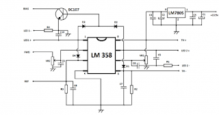
The 5V stabilizer LM7805 is there to ensure good separation, and the BC107 transistor is used to increase current capabilities on the output. Parts list:
C1 – 100uF / 16V
C2 – 470uF / 6.3V
C3 … C10 – 10nF ceramic
R1, R4 – 470 ohm
R2 – 1 Kohm
R3 – 10 Kohm
VR1, VR2 – 10 Kohm
D1 … D4 – 1N4148
The circuit will trigger once one of the two described conditions will take place, and will remain like this until power is removed for 10 seconds, due to D1 or D4 diodes. A LED connected between LED1 + and LED1 – points will signal SWR protection enabled, and a LED connected between LED2+ and LED2 – will signal thermal protection enabled. TH+ and TH- will be connected to a 1Kohm NTC thermistor wich will be placed on the heatsink, as close to the amplifier’s power transistors as possible, and the FWD and REF points will be connected to a SWR sensing board like the one described in the SWR meter article. For reliable operation, low-pass filters on both FWD and REF lines might be needed, made from a series 1Kohm resistor and a 10 uF / 16V capacitor to ground.
There are many ways in wich the amplifier might be stopped from working once these protections trigger. Switching back the RX/TX relay while in full operation might be dangerous (for a second both transmitter and amplifier will work without a load) plus the relay might be damaged. The simple way is to cut down the power of the amplifier by removing the gate bias, by simply connecting the BC107′s collector (BIAS point) to the bias voltage regulator’s reference circuit (pin 5 of MC1723CP in the Eb104 schematic). This will still allow you to remain on the air, the transmitter will see the correct impedance on the amplifier’s input and the amplifier’s finals will be able to handle even infinite SWR and the heatsink will get the chance to cool down due to running in low power mode. SSB or AM work will be a problem, because the amplifier will work in C class now.
This has been tested with 100W on both antenna and dummy load, it’s working OK, the real test will be when the rest is finished though.
Next full text...
I have developed the protection circuit for the EB104 amplifier I am working on, after I finally had some time to design and test a few models. The main requirements have been:
- protection in case of high temperature;
- protection in case of high SWR;
- protection in case of wrong output filter selection;
- simple design (i’m a fan of the whole K.I.S.S. rule of thought), able to work in strong electromagnetic fields, reliable, inexpensive.
Because i will be using the same directional coupler i have used in the SWR meter (the one made on PCB) wich is directly influenced by the signal frequency, and because i want full HF coverage, i cannot just measure the reflected signal and make a circuit cut the amplifier when it goes over a limit; on 28Mhz the coupler generates roughly 4 times more voltage that let’s say in 7Mhz. So a system that compares direct and reflected signal and triggers when the latter is percentually too high was needed, therefore an operational amplifier was the natural choice. This will solve the SWR problem, and because the directional coupler will sit between the amplifier output and the low-pass filters, it will also trigger when a wrong band is selected.
The thermal problem will be even more easy to fix, i will use a NTC thermistor in a resistive divider; the second operational amplifier from the LM358 IC I have chosen to use will just compare the voltage from the resistive divider to a preset one, and will trigger when the thermistor’s value gets too small.
As usual, it’s much easier to understand when pictured:
C1 – 100uF / 16V
C2 – 470uF / 6.3V
C3 … C10 – 10nF ceramic
R1, R4 – 470 ohm
R2 – 1 Kohm
R3 – 10 Kohm
VR1, VR2 – 10 Kohm
D1 … D4 – 1N4148
The circuit will trigger once one of the two described conditions will take place, and will remain like this until power is removed for 10 seconds, due to D1 or D4 diodes. A LED connected between LED1 + and LED1 – points will signal SWR protection enabled, and a LED connected between LED2+ and LED2 – will signal thermal protection enabled. TH+ and TH- will be connected to a 1Kohm NTC thermistor wich will be placed on the heatsink, as close to the amplifier’s power transistors as possible, and the FWD and REF points will be connected to a SWR sensing board like the one described in the SWR meter article. For reliable operation, low-pass filters on both FWD and REF lines might be needed, made from a series 1Kohm resistor and a 10 uF / 16V capacitor to ground.
There are many ways in wich the amplifier might be stopped from working once these protections trigger. Switching back the RX/TX relay while in full operation might be dangerous (for a second both transmitter and amplifier will work without a load) plus the relay might be damaged. The simple way is to cut down the power of the amplifier by removing the gate bias, by simply connecting the BC107′s collector (BIAS point) to the bias voltage regulator’s reference circuit (pin 5 of MC1723CP in the Eb104 schematic). This will still allow you to remain on the air, the transmitter will see the correct impedance on the amplifier’s input and the amplifier’s finals will be able to handle even infinite SWR and the heatsink will get the chance to cool down due to running in low power mode. SSB or AM work will be a problem, because the amplifier will work in C class now.
This has been tested with 100W on both antenna and dummy load, it’s working OK, the real test will be when the rest is finished though.
source:link
Subscribe to:
Posts (Atom)